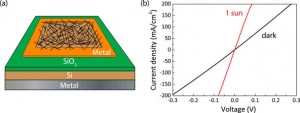
Solar energy is a topic on everyone’s mind: environmentalists, scientists and engineers, conscious citizens. New research conducted by Yale scientists reveals ways to make solar energy more efficient, starting at the level of a solar cell.

Image courtesy of Nano Letters.
The team, led by doctoral candidate Xiaokai Li and associate professor of chemical and environmental engineering André Taylor, has developed an innovative method for increasing the efficiency of electronics made of Single-Walled Carbon Nanotubes (SWNTs). SWNTs are a special type of carbon nanotube that presents advantages such as high conductivity and mobility. The new procedure consists of exposing the nanotubes to hydrogen fluoride and an electric current in order to remove oxygen molecules from the nanotubes’ surfaces. In contrast with more conventional approaches to the removal of oxygen, such as exposure to high temperatures, this method has presented outstanding results. It has already set records for high power conversion efficiencies (PCE), a measure of how efficiently a solar cell converts sunlight to electric energy.
SWNTs have many applications, from computer devices to solar cells that convert sunlight into electrical energy. Many researchers, including Li and Taylor, hope to use these recent result as a stepping stone towards more efficient carbon nanotubes, which may lead to advances in energy and computer electronics. “Carbon nanotubes are used for a variety of things, including hybrid solar cells. And our hope is that this method will drive down the cost for solar cell production,” Taylor said.
Li and Taylor worked with SWNT/p-type-Silicon (SWNT/p-Si) nanotubes, which have previously shown lower PCEs than standard silicon-type SWNTs. “We want the highest value for the PCE to reach the best performances,” Taylor said. By nearly doubling the PCE of a SWNT/p-Si nanotube, Li and Taylor’s research has greatly contributed to the development of efficient carbon electronics.
The method presented by the Yale team is innovative because it follows a unique sequence of steps. Common procedures include high temperature and ultrahigh vacuum or inert gas exposure, which provide a PCE of only 1.9 percent. Originally, the Yale scientists tried a low-temperature electric current stimulation method, which did not provide satisfactory results. However, they observed that exposure to high temperature followed by current stimulation provided record efficiency of 3.7 percent.

By applying results obtained in previous research on other devices, they designed a new approach to oxygen elimination: hydrogen fluoride treatment followed by electric current stimulation. “The reason we did the exposure to hydrogen fluoride is that we wanted to eliminate any oxide layers and get a clean interface between Silicon and the nanotubes,” Taylor said.
The new method has two components. First, the SWNT surface is treated with hydrogen fluoride vapor, leading to the removal of the oxygen molecules — a process imported from the semiconductor industry for removing oxygen from silicon surfaces. Then, a constant electric current is applied to the nanotubes to remove other residual molecules. “Even at room temperature there is a natural oxide on top of the silicon. When you have an oxide layer, it can become a barrier and decrease the performance [of the device],” Taylor said. Li and Taylor have shown that when combined, these methods substantially improve PCE values and create better nanotubes than does electric current stimulation, ultrahigh vacuum, or the traditional heating treatment applied alone.

Their paper was published in Nano Letters on November 12, 2014.
