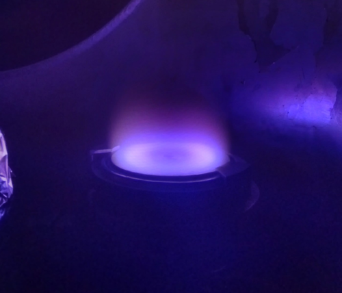
Science now allows us to replicate designs on the atomic level, thanks to a team of Yale researchers led by Udo Schwarz and Jan Schroers, professors of mechanical engineering and materials science. By using a technique called sputter deposition, this breakthrough could be practical and desirable for mass industrial use.
An efficient way to reproduce nanostructured surfaces could have a huge impact on areas of technology such as high-density data storage, photonic devices, water filtration, and electrodes in fuel cells. Imprinting doesn’t require the use of a clean room—a tightly regulated space of filtered air that minimizes possible contaminants—which typical nanomanufacturing requires. The material used to imprint, metallic glass, also has useful properties of durability and strength. “We had the question: What’s the limit of this? If I can do this to thirty nanometers, is there anything that stops us?” Schwarz said.
The key to atomic scale replication is the use of bulk metallic glass, also known as amorphous metal—a material made by cooling a liquid metal alloy so quickly that the atoms don’t have time to arrange themselves in a crystalline structure and instead lie jumbled together. Without a crystalline structure, the researchers found that the only factor limiting the size of what they could replicate was the size of the atoms and the distance between them. The random configuration of atoms in a metallic glass gives it a viscous quality, allowing it to be blown just like glass, or molded onto nanostructured surfaces. It can be processed as plastic, but unlike plastic, it is very hard, resistant to wear and tear, and able to conduct electricity.
Once the researchers had shown that there was no limit to the size of replication except the atoms themselves, they turned their attention to scaling up the process and making it more efficient. Instead of pressing the metallic glass to the mold in a process called thermoplastic forming, the researchers used a technique called sputter deposition, which doesn’t require high heat or pressure. They shot argon ions at a metal plate, which loosened the surface atoms and sent them falling onto the mold below. As single atoms, they cooled immediately upon hitting the room-temperature mold to form a metallic glass on the surface.
“If you use, for instance, just gold, then it will still crystallize, so you still need the right combination of different metals,” Schwarz said. “The trick is to basically have small atoms and large atoms together so they don’t line up nicely in a crystal, and [since] they don’t know what to do, they just stick in the glass.”
Sputter deposition makes it possible to use many more metallic alloys than thermoplastic forming can for nanoscale imprinting. The researchers theorize that hundreds of millions of different combinations of metallic elements could be possible when using sputter deposition, while thermoplastic forming only allows hundreds.
“If you want to do thermoplastic forming, there are some restrictions on the mold, on the alloy that you can choose, and some specific conditions that you have to achieve—[like] the temperature or the pressure to do the thermoplastic forming,” said Zheng Chen, a graduate student who worked on the study.
Because sputter deposition doesn’t require high heat and pressure, any material that doesn’t react with the metallic glass could potentially be replicated. For example, biomaterials acting as molds are a potential application for this technology. “We think you can now duplicate anything you really want at the atomic scale,” Schwarz said.
Schwarz hopes to pursue a project to find a way to keep sand and dirt off of solar panels by reproducing the structure of snakeskin, which has unique nano-scale patterns that force sand to slide off. To do this, Schwarz wants to first make a mold with metallic glass, then copy the pattern onto plastic. Another possible project is to use nanoimprinting with metallic glass to reproduce nanostructured surfaces that can act as catalysts for clean energy reactions. These reactions can be applied to areas like jet fuel.
“Maybe it never goes anywhere, maybe metallic glasses are totally bad. But because people haven’t tried yet, there are a lot of intriguing things that could happen because of the disorder [of the atomic structure],” Schwarz said.
Works cited
1. Zheng Chen, Amit Datye, Georg H. Simon, Chao Zhou, Sebastian A. Kube, Naijia Liu, Jingbei Liu, Jan Schroers, and Udo D. Schwarz. (2020). Atomic-Scale Imprinting by Sputter Deposition of Amorphous Metallic Films. ACS Applied Materials & Interfaces 12(47), 52908-52914. DOI: 10.1021/acsami.0c14982.
2. Chao Zhou, Amit Datye, Zheng Chen, Georg H. Simon, Xinzhe Wang, Jan Schroers and Udo D. Schwarz. (2020). Atomic Imprinting in the absence of an intrinsic length scale. APL Materials 8(11), 111104. DOI: 10.1063/5.0027982

